Patexia is offering a $5000 prize to the winner of a research contest involving charge pumps in voltage controlled oscillators. The goal is to find relevant, published material pre-dating a certain patent. This is a chance to win money, to tackle a real problem, to showcase your technical skills, and to gain visibility in the industry (maybe).

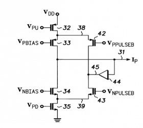
One of the key features of this design is the presence of a charge conduction path (transistors 42 and 43 in the following circuit diagram) to discharge the parasitic capacitance of nodes 38 and 39 into the discharge node of 45 and as a result reduce the error current in the output. The charge conduction path is enabled only on one transition edge of the input pulse and is disabled on the other transition edge of the input pulse to isolate the node from the output.
